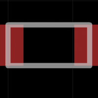
A package is a physical layout of the component, e.g. resistor, you are trying to create. This layout includes the dimensions of the part itself and the dimensions of the copper pads. With this information, a 2-dimensions CAD representation can be created in Eagle software, which will then be placed on the PCB.
In a previous tutorial, I discussed how to create a symbol for a library in Eagle. Now, I will discuss how to create a corresponding package for that same symbol, a resistor. Note that a symbol and package go hand-in-hand as discussed in a previous tutorial. Let’s begin
What will you learn in this tutorial?
The table of contents shows the topics you will learn in this tutorial.
[toc]
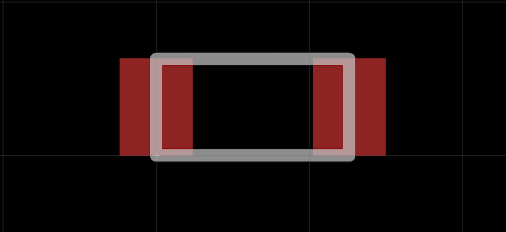
The final outcome of today’s tutorial is shown in Figure 1 below. This is a 2D CAD layout of a 0603 surface mount resistor. Keep reading to learn how to create this package in Eagle.
Requirements for Creating a Package
The most important requirement is the datasheet of the part itself. This datasheet will show the dimensions of the part. You will use these dimensions to create a 2D representation in Eagle.
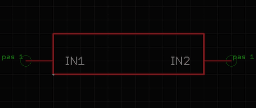
Another important requirement is a symbol of the part, which I discussed how to create previously. However, you can create a package before a symbol but I like to first create a symbol then a package because it is more intuitive. You can see the symbol I created in Figure 2 on the right.
How to Create a New Package File
Before creating a package, a library must exist to where you can save the package. After you have identified the library where you will be working from, follow these steps:

Menu procedure
- Click on Library -> Package
- Enter in a name of the package in the New box.
- Click OK to save
You can also create a package using the shortcut options available in the top toolbar shown in Figure 3. If you choose the shortcut method, you need to still perform steps 2 and 3 to name your part.
Reading Datasheets for Package Design
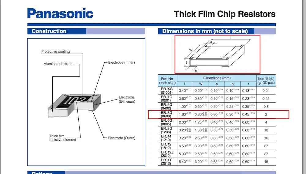
The datasheet includes necessary information for the layout of the part on the actual PCB. In this tutorial, I will design a 0603 resistor and thus I obtained a datasheet from Panasonic series of resistors. Figure 4 below shows in red boxes the specific dimensions we are interested in.
Specifically, We need the length of the resistor (1.60 mm), the width (0.80 mm), and finally, the length of the copper pad (0.30 mm).
For other parts, e.g. ICs, you will need not only the width and length of the IC itself, but also the length/width of a lead and spacing between leads.
How to Draw the Package
Now that we created a package file and obtained the dimensions, we can draw the resistor package. The industry standard is to provide dimensions in millimeters as opposed to Eagle’s default settings in inches. The first thing we need to do is change the grid measurements.
Changing Grid Measurements
The grid is shown in the window by lightly-colored squares. Each square is a unit by a unit. The default measurement of the unit is 0.1 inches by 0.1 inches. However, I like to change this to 0.1 mm to 0.1 mm. This is the case because when we measure 1.6 mm as the length of the resistor, I know that I exactly need 16 boxes.
Change the grid measurements to 0.1 mm by 0.1 mm so it is simple to draw the components
To change the grid measurements, follow these steps:
- Make sure you have a package file created
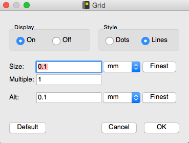
- Click on View -> Grid
- Display options set to ON and style option set to Lines
- In the size box, enter 0.1 and choose mm
- In the alt box, enter 0.1 and choose mm
- Click OK
The outcome of the above steps are shown in Figure 5 below.
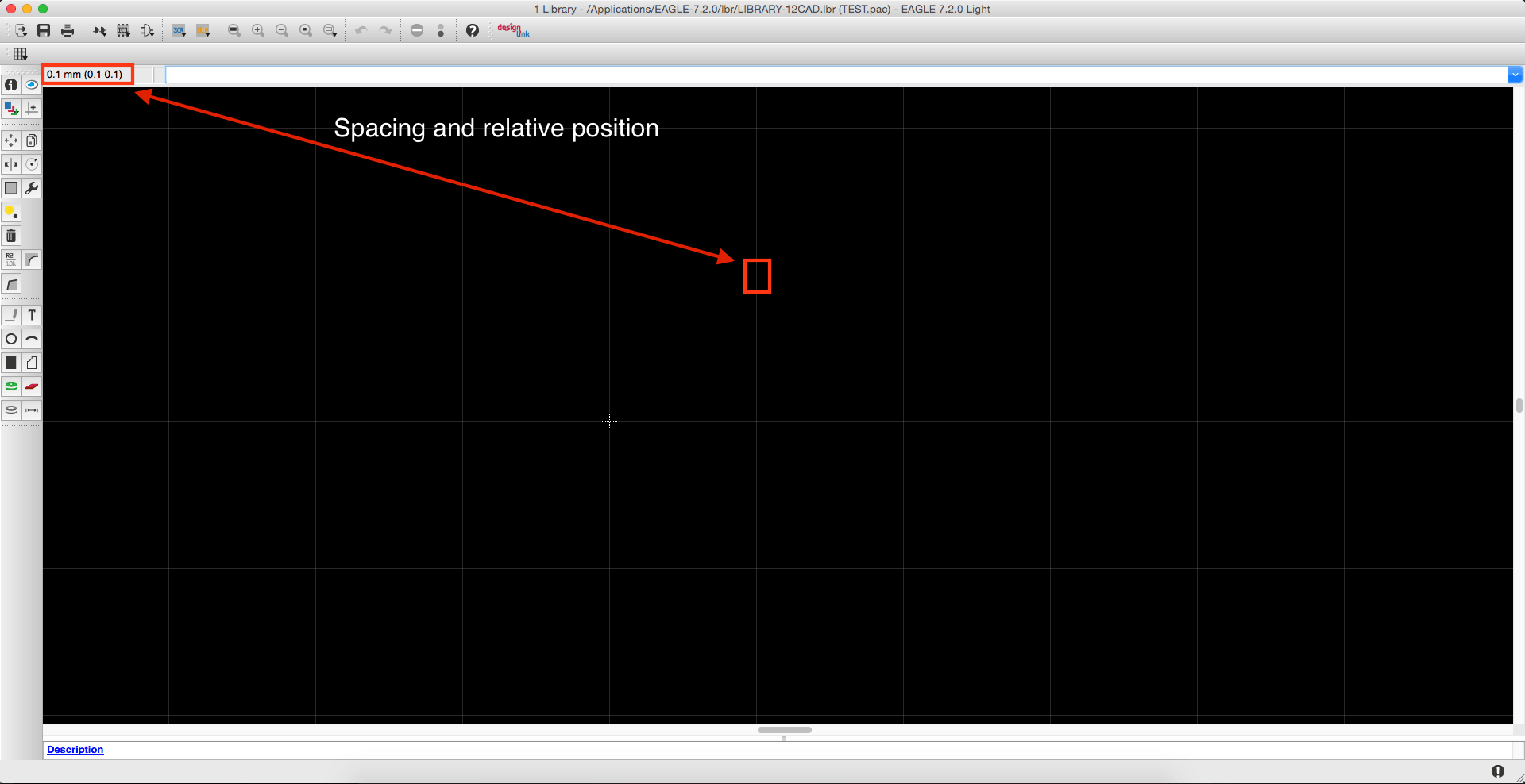
After changing the grid measurements, you can verify it works by using your mouse cursor. Point your mouse cursor on the edge of a certain box and look at the top left for the precise measurements. It should say 0. 1 mm (X, Y) where X and Y are the relative positions. An example of this is shown in Figure 6 below.
Draw the Outline of the Part
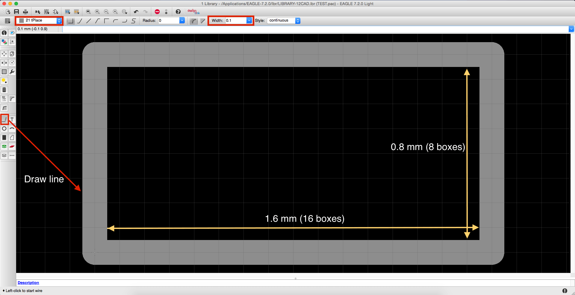
I like to create an outline of the part. In the case of the resistor, this will be a rectangle with length 1.6 mm and width 0.8 mm. This outline make it much easier to double-check your work.
- Click Draw Lines option in the left toolbar
- In the new top toolbar, change to “21 tPlace” (if not already selected)
- In the new top toolbar, change width to 0.1
- Draw 4 segments for the rectangle. Length is 1.6 mm (16 boxes) and width is 0.8 mm (8 boxes)
- Press escape key (ESC) to stop drawing
In step 2, the menu should be changed to 21 tPlace because tPlace is an outline for visualization. The final outcome as well as where each of these options are located is shown in Figure 7 below.
How to Add Copper Pads to the Package
Since I created an outline, it will be simpler now to add copper pads. A copper pad is the spot where the resistor will be attached to the PCB by solder. Without this, no electricity flow can occur.
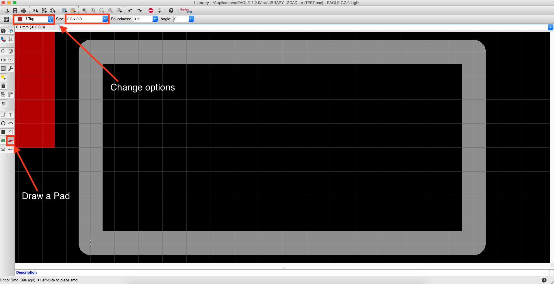
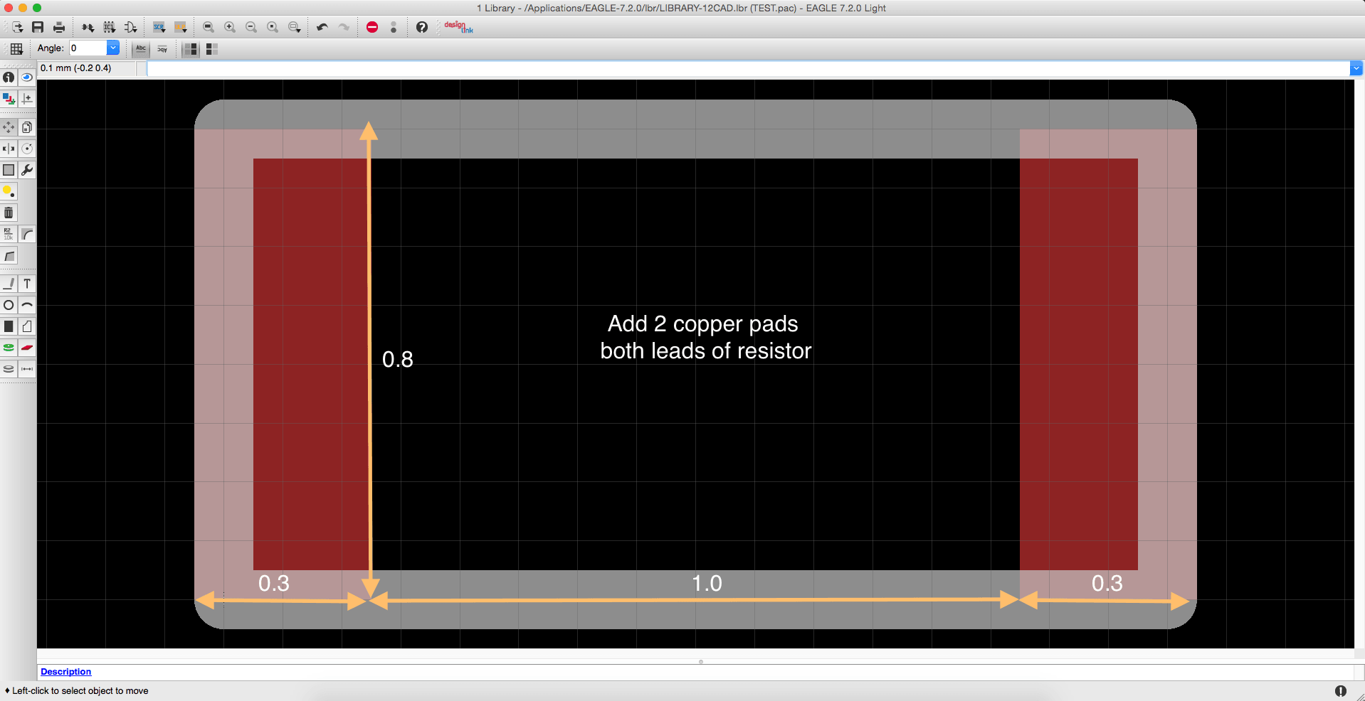
For the 0603 resistor, we need to create two copper pads. Each pad will have a length of 0.3 mm (3 boxes) and width 0.8 mm (8 boxes). The pads will start from the left and right edges of the outline.
- Click on the ‘Draw a surface mount pad‘ option in the left toolbar
- In the new top toolbar, change the menu option to ‘1 Top‘
- In the new top toolbar’s box for size, change default values to 0.3 x 0.8
- Place the pad on the left/right edges of the outline
These steps can be seen visually in Figure 8 below:
After adding the copper pads at the specific locations, the package should look similar to Figure 9 below. Make sure the dimensions are correct. Make sure the pads are designated for the top layer (step 2). If everything checks out, the package is complete. Go ahead and save it!
Optional Changes to the Package
The following tricks are optional but highly recommended for creating a package in Eagle.
Increase the Copper Pad Size for Easy Soldering
If you look closely at Figure 9, the copper pads actually sit directly below the resistor. How would you solder the resistor to the board? It is too difficult to solder with the current dimensions.
The best fix for this is to increase the copper pad’s length by twofold, i.e. 0.6 mm instead of 0.3 mm. This will give you enough room to solder the resistor.
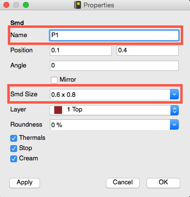
- Right-click on the copper pad and go to Properties
- Change the SMD Size option from 0.3 x 0.8 to 0.6 x 0.8
- Click OK
- Pad may shift out of place. Make sure 0.3 mm (3 boxes) is always under the outline
Changing the Name of Copper Pads
To avoid confusion, each pad should have a meaningful. For example, if a pin is indicated to be GND in the datasheet, then by all means name it GND. In the case of the resistor example, I named the pads P1 and P2. Follow these steps:
- Right-click on a pad. Go to Properties.
- Change the name box to something descriptive
See Figure 10 above for more details.
Video Tutorial on How to Create a Package in Eagle
The video tutorial will show the step-by-step process with a bit more detail. I recommend for you to take a look at it.
https://www.youtube.com/watch?v=FgzIy2kyQFQ
Final Thoughts
In this tutorial, I covered how to create a package in Eagle software using the resistor symbol we already created. After this tutorial, you should be able to create a package file, change the grid measurements to make Eagle easy to use, create an outline of the part, and lastly, add copper pads. The last remaining step for creating your own part in Eagle is to take the symbol and the 2D CAD representation of the part to create a device, which is covered in another tutorial.
Did you have any difficulties with this tutorial? Please share your thoughts and/or difficulties by leaving a comment below.

