When designing a PCB in Eagle CAD software, the libraries available to you may not have the components you require. In this situation, you will need to create your own library in Eagle with the necessary parts. In this tutorial, I will show you how to create a new library and a new symbol. A symbol is the schematic representation of your part, which includes the input and/or output signals, e.g. voltage, as pins.
First, I will discuss how Eagle manages new parts. Then, I will layout the procedure to create a new library. Finally, I will show you how to design a symbol using a SMD resistor as an example.
What will you learn?
The table of contents below explains the various topics covered in this tutorial to teach you how to create a new symbol in a library.
[toc]
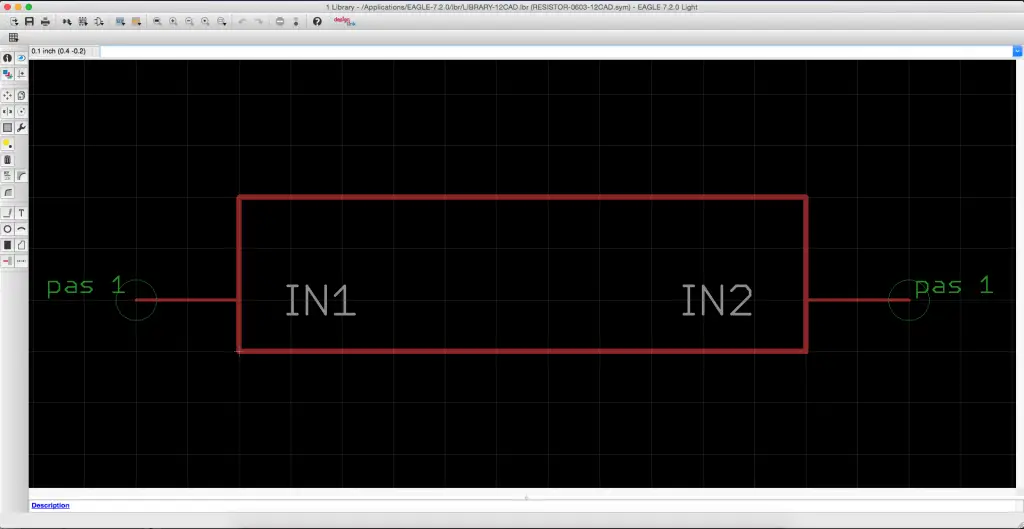
Before we begin, the final outcome of this tutorial is shown below. In this tutorial, we will create a symbol of a resistor. However, the procedures can be applied to any part you wish to create.
Why are Parts Important?
Without a part, you cannot create the schematic, which in turn, means you cannot create the PCB layout. Eagle has a three aspects to each part. These are:
- Symbol
- Package
- Device
The symbol is the schematic representation and does not need to follow any dimensions or shape. As you will see, in my example, I represent a resistor as just a square box with two pins. The package is the actual physical layout drawn via 2D CAD and requires dimensions obtained from datasheets.
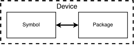
Creating a device allows Eagle to combine a specific symbol to a specific package. The symbol’s corresponding pins and the package’s corresponding pads need to be matched. The interaction is visually shown in Figure 1.
In this tutorial, I will create a symbol of a resistor. In the next tutorial, I will create the package for a 0603 resistor which the symbol will represent. The device will be created in the third tutorial where the package and symbol will be combined. Let’s begin this tutorial.
How do I Create a Library?
In the control panel of Eagle PCB, a list of all available libraries are visible. We want to add a new library to this list. To do so, follow these steps:
- Go to File -> New -> Library
- A new window will open.
- Go to File – Save As -> Enter a name (extension .lbr) -> Click Save
Create a NEW Symbol in Eagle Library
Now that a library is created, we can create a symbol. To create a NEW symbol, you can either use the menus as explained in the steps below or the toolbar as shown in Figure 2.

Menu procedure
- Click on menu Library -> Symbol
- Enter a name in the new box for your symbol
- Click OK
If you choose the process shown in Figure 2, a window will appear where you can give the symbol a name (follow steps 2 and 3 above).
How to draw a Symbol
Once the previous step is complete, you will see a new toolbar available on the left side of eagle with several options, e.g. Wire, Pin, among others. Now, we can begin drawing the symbol.
The symbol can be any shape and size. For example, a resistor can be a box, or a circle, or any other shape.
To draw a symbol, follow these steps:
- Click on Wire (draw lines) option on the left toolbar
- Click on the window and create a shape with closed edges
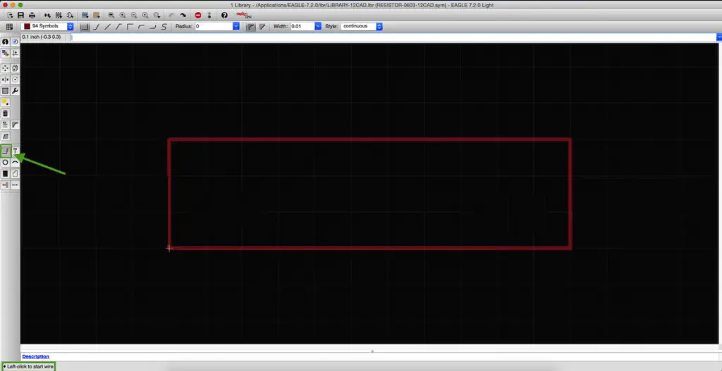
I chose to draw a rectangle for a resistor. You can see the location of the Wire option and the outcome after using it in Figure 3 below.
Once you have successfully created a shape similar to the one above, you can continue by adding pins to it.
Adding Pins to the Symbol
Without pins, the symbol is unaware how many electrical connections are present. For a resistor, we know there will be two pins representing the two leads.
To add a pin, follow these steps:
- Click on the Pin option (draw a pin)
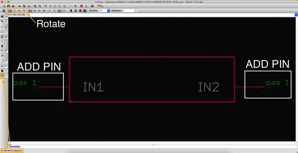
- Rotate the pin from the top toolbar, if required (See Figure 4)
- Click on the symbol to place the pin
- Repeat steps 1 to 3 for additional pins
Figure 4 below shows this process.
Editing properties of Pins
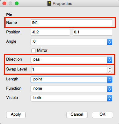
Now that the pins are added, we need to edit the properties. Most importantly, we need to give the pins a descriptive name, change the direction, and change the swap level. I chose to name one of the pins IN1 and other IN2.
1. Direction property
The direction is required for the Electrical Rule Check (ERC) in order to validate the connections in your PCB schematic. This dropdown menu has several options but the most commonly used ones are:
- IO: represents an input or output
- IN: represents an input
- OUT: represents an output
- PWR: represents a pin that receives voltage to power the device
- PAS: represents a pin that passes the signal (e.g. used for resistors, capacitors, etc)
Since we are modelling a resistor, we will choose PAS for both of the pins. However, if you are working with integrated circuits (ICs), then majority of the pins will be IO, IN, or OUT.
2. Swap level property
The swap level indicates if pins can be swapped. For resistors, we know that the connection to the pins are irrelevant and thus pins can be swapped. A swap level of zero (0) indicates no swapping. On the other hand, a swap level of more than 0 indicates swaps can occur. I set the swap level value to 1 for both pins. See Figure 5 below for the chosen properties for pin IN1.
For other parts, e.g. ICs, make sure to study the datasheet to determine the different pin functions and then change direction and swap level properties accordingly.
Video Tutorial
To further clarify this tutorial, watch the video below for a detailed step-by-step procedure. This video only covers the creation a library and a new symbol. Creating the package and the device will be covered in other tutorials.
Final Thoughts
In this tutorial, I discussed how to create a library to eventually create your own symbol. The topics covered included creating a library, creating and drawing a symbol, and finally, adding pins and changing their properties. To illustrate the procedure, I applied the steps to create a resistor, however, this approach can be applied to any part. If you tried this tutorial on a different part, it would be great if you could describe or even better share your creation. Leave a comment below!
In the next tutorial, I will cover how to create a package that resembles the physical dimensions of the resistor.
Check out the other available tutorials here.
Did you have any difficulties with this tutorial? Please share your thoughts and/or difficulties by leaving a comment below.


Comments
One response to “How to Create a NEW Symbol in a Library – Eagle PCB”
Awesome. Really helpful. Thanx a lot!